RFLA1022
RFLA1022 is High Linearity Amplifier manufactured by RF Micro Devices.
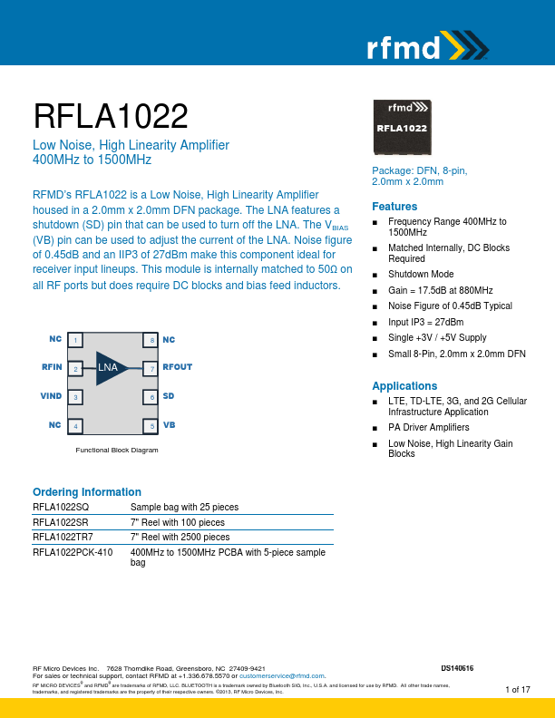
features a shutdown (SD) pin that can be used to turn off the LNA. The VBIAS (VB) pin can be used to adjust the current of the LNA. Noise figure of 0.45d B and an IIP3 of 27d Bm make this ponent ideal for receiver input lineups. This module is internally matched to 50Ω on all RF ports but does require DC blocks and bias feed inductors.
NC 1
8 NC
RFIN 2 LNA
7 RFOUT
VIND 3
6 SD
NC 4
5 VB
Functional Block Diagram
RFLA1002
Package: DFN, 8-pin, 2.0mm x 2.0mm
Features
- Frequency Range 400MHz to 1500MHz
- Matched Internally, DC Blocks Required
- Shutdown Mode
- Gain = 17.5d B at 880MHz
- Noise Figure of 0.45d B Typical
- Input IP3 = 27d Bm
- Single +3V / +5V Supply
- Small 8-Pin, 2.0mm x 2.0mm DFN
Applications
- LTE, TD-LTE, 3G, and 2G Cellular Infrastructure Application
- PA Driver Amplifiers
- Low Noise, High Linearity Gain
Blocks
Ordering Information
RFLA1022SQ
Sample bag with 25 pieces
RFLA1022SR
7" Reel with 100 pieces
RFLA1022TR7
7" Reel with 2500 pieces
RFLA1022PCK-410 400MHz to 1500MHz PCBA with 5-piece sample bag
RF Micro Devices Inc. 7628 Thorndike Road, Greensboro, NC 27409-9421 For sales or technical support, contact RFMD at +1.336.678.5570 or customerservice@rfmd..
DS140616
RF MICRO DEVICES® and RFMD® are trademarks of RFMD, LLC. BLUETOOTH is a trademark owned by Bluetooth SIG, Inc., U.S.A. and licensed for use by RFMD. All other trade names, trademarks, and registered trademarks are the property of their respective owners. ©2013, RF Micro Devices, Inc.
1 of 17
Absolute Maximum Ratings
Parameter Supply Voltage Control Voltage DC Supply Current Power Dissipation Max RF Input Power Storage Temperature ESD Rating (HBM) Moisture Sensitivity...